In recent years, photonic devices are becoming increasingly miniaturized and integrated due to the continuous advancement of various micro- and nanofabrication technologies and the rise of planar optics. Innovative products such as superlenses, superlattice polarizers, and superlattice spectrometers have attracted more and more attention, revolutionizing the field with their excellent performance and small size. However, most photonic devices are fixed and monolithic in their functionality once fabricated, making them difficult to adapt to changing application requirements.
Researchers have proposed the concept of tunable optics, which aims to dramatically improve the functionality and utility of optical devices by adjusting its characteristics to suit different scenarios. There are various methods and technical materials to achieve ‘tunability’, each with its own merits. Liquid crystal materials, known for their wide range of applications in displays, are capable of achieving quasi-continuous phase and intensity modulation, but its slow modulation rates and limitations related to polarization restrict further application. Devices based on electro-optic effects and carrier injection stand out for their ultra-high operating bandwidth, although their modulation depth needs to be improved. On the other hand, electrochemical methods and phase change materials have been noticed by researchers with larger intensity modulation capabilities, but their performance in terms of speed and lifetime remains unsatisfying. Microelectromechanical systems (MEMS) are marked with excellent modulation depths and switching rates, but complicated to fabricate.
Recently, Dr Sailing He, Professor of College of Optical Science and Engineering, Zhejiang University, Adjunct Professor of Shanghai Institute for Advanced Study, Zhejiang University and his team proposed a versatile solution with a high-speed tuning rate, long-life durability and programmability across multiple pixels remains elusive. They introduced a programmable nanophotonic matrix consisting of vanadium dioxide (VO2) cavities on pixelated microheaters that meets all these requirements. The indirect Joule heating of these VO2 cavities could result in pronounced spectral modulation with colour changes and ensured exceptional endurance even after a million switching cycles. Precise control over the thermal dissipation power through a SiO2 layer of an optimized thickness on Si facilitated an ultrafast modulation rate exceeding 70 kHz. The authors further demonstrated a video-rate nanophotonic colour display by electrically addressing a matrix of 12 × 12 pixels. Furthermore, inspired by the unique pixel-level programmability with multiple intermediate states of the spectral pixels, a spatiotemporal modulation concept w
as introduced for spectrum detection.
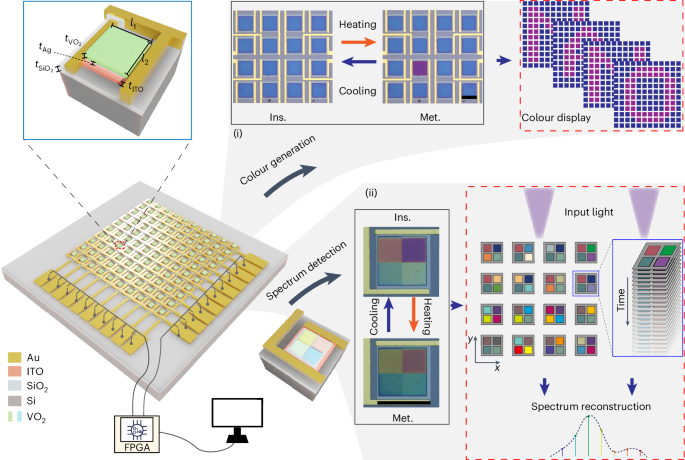
The schematic diagram for the nanophotonic pixel matrix, controlled with an FPGA and computer
The as-prepared VO2 material was first characterized, displaying a typical hysteresis effect with a low operating temperature in the device. Various lossy cavities with different thicknesses of the VO2 layer were then fabricated. By varying the thickness of the VO2 layer, a full gamut accounting for 40% of standard red–green–blue (sRGB) colour space could be obtained. The spectra of all intermediate states have been measured multiple times, and the device could achieve stable intermediate-state colours and spectra under the same temperatures or voltages. The authors observed over 60 intermediate-state levels at a wavelength where the reflectance variation range was large. The device can also work as an intensity or spectrum modulator.

The phase change performance of the VO2 cavities
An important aspect of a dynamic device is the modulation bandwidth, especially for, for example, free-space communication, endoscopic bio-imaging and beam steering applications. In electronic devices, the switching speed of VO2 microstructures could reach picoseconds, attractive for tunable optical devices. However, in photonic devices, hindered by the large volume of the devices, even a tens-of-kilohertz rate was hard to reach. To better explore the factors for switching speed, the authors considered both heating and cooling times.
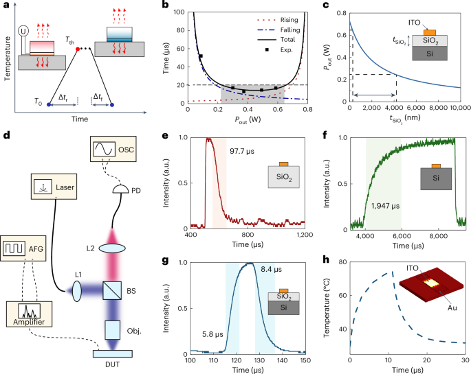
The optimization for the electrothermal response speed of the VO2 cavities
To further validate the frequency response of the device, the authors carried out modulation measurements on the sample by the logarithmic increase of voltage-biased switching frequency, from 100 Hz to 100 kHz, with a total sweep time of 10 s. This ultra-long lifetime observed was mainly attributed to the low threshold temperature of VO2 devices, alleviating the burden for a microheater to trigger the phase transition. For the present device, the trigger current for the phase transition was around 37.5 mA.
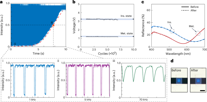
The dynamic response and the life cycle of the VO2 cavities
The authors adopted a row–column addressing scheme to achieve programmable control of the 12 × 12 pixels for a prototype structural colour display. In addition to the high-speed response, based on the hysteresis effect of VO2, the authors also demonstrated a non-volatile display. The whole device was first placed on a hotplate at ~54 °C. Then a 1.1 V pulsed signal was applied to some of the pixels to trigger the phase transition process. Due to the hysteresis effect, the pixels with a voltage on underwent a different colour change.
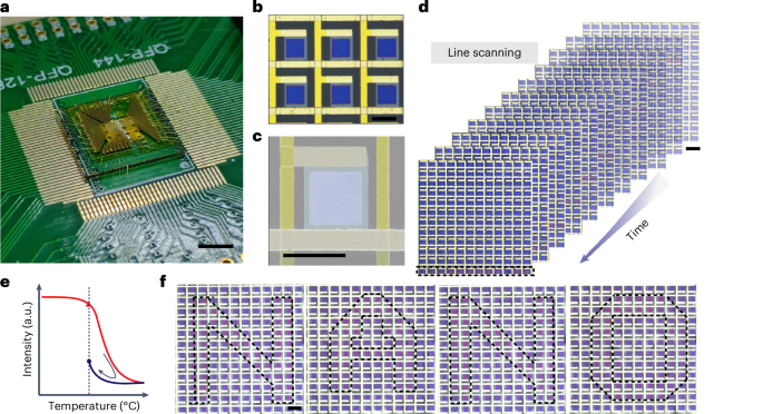
Demonstration of a structural colour display
To show its versatility, the programmable matrix of spectral pixels was then employed for spectrum detection. By harnessing the multiple intermediate states and the pixel-addressing feature of the matrix, the authors tackled the trade-off of enlarging the footprint or deteriorating the detection performance with a unique spatiotemporal modulation scheme. The design approach involves integrating 2 × 2 VO2 tunable filters on a single ITO heater to form a unit pixel as shown below. The pixelated tuning feature combined with multiple states provides versatile strategies for spectrum detection with flexible degrees of freedom over the spatial, spectral and temporal domains. For snapshot mode detection, sixteen unit pixels with each pixel triggered at a unique intermediate state are employed, enabling a real-time overview of the input spectral content through the reconstruction process. For tuning mode detection, a single unit pixel is cycled through various intermediate states, allowing for a fine-tuned spectral response with an ultracompact footprint.
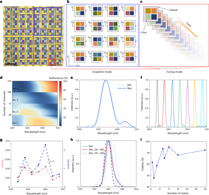
Spectrum detection through spatiotemporal modulation
In conclusion, the authors have demonstrated a video-rate nanophotonic display with VO2-based active pixels and introduced a unique spatiotemporal modulation for spectrum detection. By further optimizing the thermal capacity along with an advanced driving scheme, the device has the potential to operate in megahertz regimes. As the matrix size increased, the increasing number of sneak current paths would lead to substantial waste power dissipation for the structural colour display. Moreover, the thermal cross-talk between adjacent pixels also required careful consideration. Transistors could be incorporated into the pixel to improve the selectivity and suppress the sneak path effect, particularly in high-power-consuming devices. As for spectrum detection, the current prototype used an 8 × 8 matrix of active spectral pixels, which could be expanded to a larger scale with the more sophisticated read-out circuits widely used in current image sensors. With megapixels, one could achieve an on-demand spectral imaging system, by customizing the region of interest with the hybrid strategy of snapshot mode and tuning mode. With a more complicated design strategy, the spatiotemporal filter could also work in transmissive mode or be extended to infrared bands. Due to its compatibility with present-day Bayer filters, the spatiotemporal concept was expected to generate new detection architectures for imaging and sensing applications by adapting other active platforms such as two-dimensional (2D) materials, liquid crystals and semiconductors. This enabled many programmable devices that have customized requirements, such as multifocal lenses, biomedical sensing and imaging, high-speed and solid-state optical switches, video displays and light detection and ranging.
The work was published as “Durable and programmable ultrafast nanophotonic matrix of spectral pixels” in Nature Nanotechnology, and was funded by National Key Research and Development Program of China, National Natural Science Foundation of China and the Special Development Fund of Shanghai Zhangjiang Science City etc. To access the article please go to https://www.nature.com/articles/s41565-024-01756-5.

